Current Topics
The ability to assemble nanostructures with unique and specific properties is a key technology for developing next-generation devices. For this goal, major success is anticipated through the bottom-up approach: namely, the attempt to create such nano-devices from the atomic or molecular level instead of miniaturizing from the macroscopic world. In the bottom-up approach, the ultimate is to fabricate artificial nanostructures on surfaces by manipulating single atoms or molecules one by one.
In our laboratory, we are developing such atom manipulation techniques as well as chemical identification and local characterization techniques using scanning probe microscopy (SPM). Our SPMs are based on atomic force microscopy (AFM), which has wide applications including insulator imaging and force measurements. Combining SPM with scanning tunneling microscopy (STM) allows us to access various physical/chemical quantities on identical atoms at the same time. We are also developing a new system to achieve higher spatial resolution and higher functionality.
【Clarification of relationship between electric current and chemical bonding force】
【Chemically reactive probe tip plays role in moving atoms at room temperautre】
【Osaka University Prospectus 2012 p.6-7】
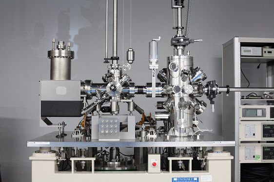
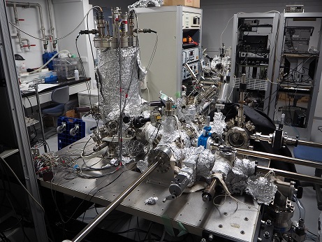
Instruments in our lab.
- UHV room temperature AFM/STM (UNISOKU custom-built)Optical interferometer cantilever deflection sensor.
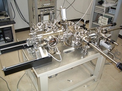
- UHV low temperature AFM/STM (UNISOKU custom-built)Optical interferometer cantilever deflection sensor.
- UHV low temperature AFM/STM (Omicron LT)qPlus type deflection sensor.
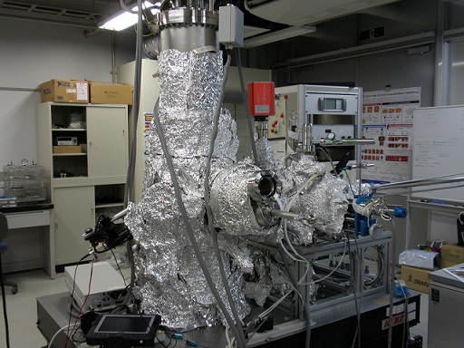
- UHV low temperature high-magnetic field SPM (UNISOKU custom-built)